Solid Quantum Sensors
NV center
Nitrogen-Vacancy (NV) center is a point defects consisting of nitrogen (N) and vacancies (V) formed in the diamond. In this system, a quantum state is maintained even at room temperature and atmospheric pressure. The quantum state of NV center could be confirmed by spin dependent fluorescence. NV center could be used as a highly sensitive sensor by detection of the changes in the fluorescence, corresponding to a change in the energy level due to magnetic field, electric field, and temperature. By controlling the number of NV center, application to various fields from nanoscale targets such as cells and molecules to macroscale targets such as biomagnetic fields are possible.
Ultrahigh sensitivity quantum magnetic sensor
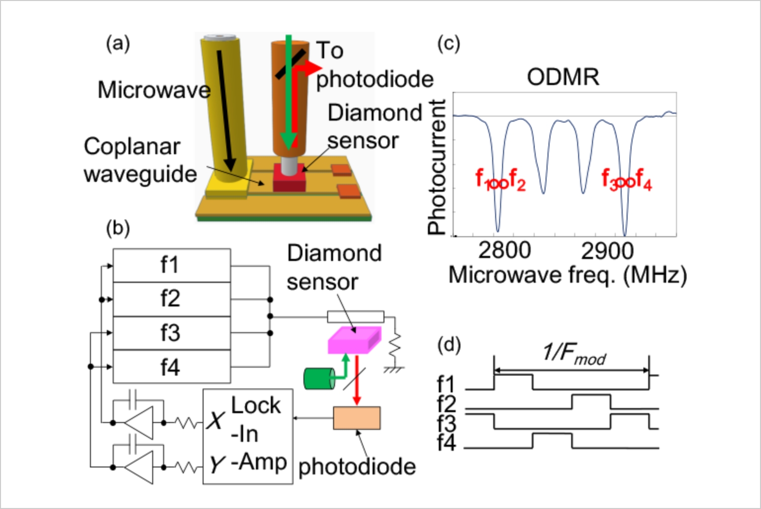
The NV center shows shift in the resonance frequency of the quantum state due to Zeeman splitting. The amount of shift in the energy depends on the intensity of the applied magnetic field. The magnetic field detection could be performed using this property.
As the number of NV centers that contribute to the magnetic field detection increases, the magnetic sensitivity improves. Therefore, the femto-tesla level sensitivity required for medical applications at the room temperature can be anticipated by using a high-density NV center.
Our laboratory aims to realize an ultra-sensitive magnetic sensor by synthesizing a highly sensitive NV centers in thin film, manufacturing a microwave circuit, and introducing a noise cancellation system.
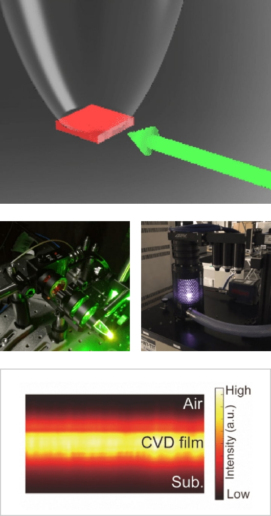
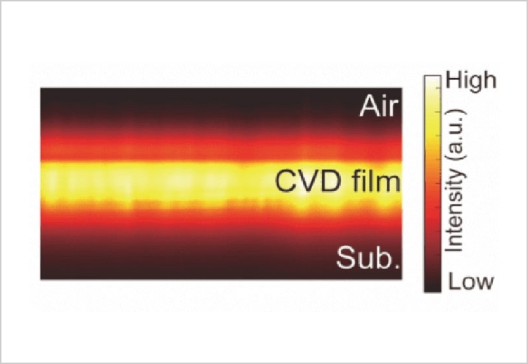
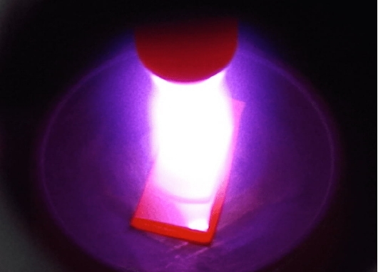
The NV centers in thin films are synthesized by chemical vapor deposition (CVD).
Since the NV center is created in the diamond lattice, it has four possible axial directions for formation.
By using CVD, the axial direction of the NV centers can be controlled in one direction, and the sensitivity for magnetic field detection can be improved.
In our laboratory, we have a technique to form a high density, perfectly aligned NV centers in thin films. And we utilize these special films to conduct a research for an application to ultra-sensitive magnetic sensors.
Quantum sensor for biomagnetism
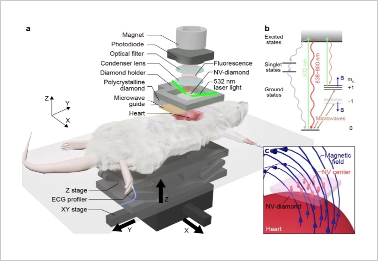
Diamond quantum sensors are expected for biological applications. For example, in the measurement of magnetoencephalography (MEG), the diamond quantum sensor can be used to reduce the size and price of the equipment. For MEG application of diamond quantum sensor, we are working on establishing MEG measurement method using NV center and improving magnetic field sensitivity.
MEG measurement using the NV center is the world’s first attempt. We have succeeded in measuring magnetocardiography (pT~nT), a magnetic field larger than magnetoencephalography (~ fT). However, there are many more engineering challenges to achieve MEG measurements, such as the structure of diamond sensor, laser irradiation method, and fluorescence detection method.
We apply advanced quantum manipulations to electron spins in NV centers to improve magnetic field sensitivity. We can build proper quantum manipulations by understanding the microscopic behavior of electron spins and photons. It is expected that this technology can approach the magnetic field sensitivity to the quantum measurement limit.
Integration EV battery monitor
集積化、電気自動車の電池モニタ
Diamond quantum sensors are expected to support electric vehicles. The diamond quantum sensor, which operates at room temperature, enables high-sensitivity magnetic field measurement even in the car. High-sensitivity magnetic field measurement using a diamond quantum sensor enables highly accurate observation of the battery usage of an electric vehicle and extends the mileage of the vehicle. In order to realize an in-vehicle diamond quantum sensor, we are researching miniaturization of sensor systems and high sensitivity in the in-vehicle environment.
The sensor system aims to be on-chip ultimately. We are working to reduce the size of the system by extracting only the functions required for in-vehicle sensors from conventional system. Furthermore, by designing microwave circuits and integrated circuits for digital processing, we will realize on-chip diamond quantum sensors.
The miniaturization and low power consumption of the sensor are required in the vehicle. These limit the sensitivity of the sensor. We are trying to increase the sensitivity of in-vehicle sensors by improving the collection efficiency of fluorescence and introducing advanced quantum measurement.
Nanoscale sensing of condensed matter physics
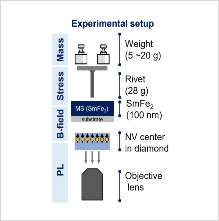
In order to increase the value of diamond quantum sensors, it is important to open up new application fields. Then, we focused on the interdisciplinary research of condensed matter physics and NV center-based sensing. Specifically, we are taking aim at developing hybrid weight imaging combining magnetostrictive materials, strain-sensitive magnetic materials, and NV centers. We focused on weight-into-magnetic field conversion of magnetostrictive materials and the high-sensitivity magnetic field imaging of NV centers. It is expected to realize imaging of small weights such as cells.
Device quantum sensing
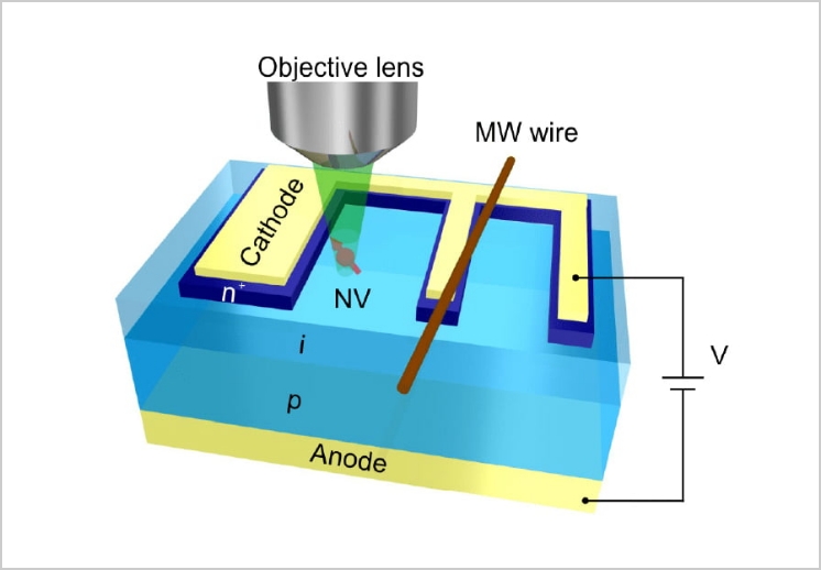
Wide-bandgap materials such as diamond shows a great potential as a next-generation material for the low-loss power electronics applications.
Although the power devices are required to be operated at high-voltage and high-temperature environment, detection of local electric field and temperature in the devices remains a challenge.
Our research aims to develop sensing-techniques to measure the physical quantities in the power devices at nano-scale region by utilizing the NV centers.
Heteroepitaxial diamond growth
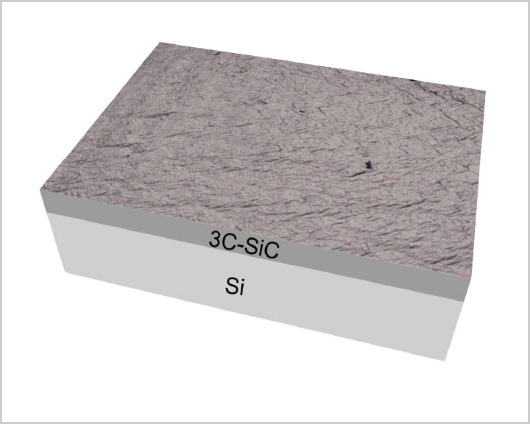
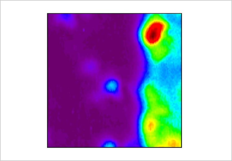
Single-crystal diamond substrates used in quantum sensors and power devices are fabricated using high-temperature and high-pressure synthesis (HPHT) methods or chemical vapor deposition (CVD) methods. These growth techniques impose limitation on the fabrication of a large area substrate to few millimeters square.Technology for synthesizing diamond in large area is indispensable for the practical applications of diamond sensors and electronic devices in the industry. In our laboratory, heteroepitaxial growth is performed on silicon substrates.
Highly oriented diamond thin films are produced on 3C-SiC / Si substrates using a uniquely developed high-density microwave plasma CVD system.High-quality diamond thin films can be synthesized on the 3C-SiC / Si (001) substrates and we have successfully demonstrated highly oriented thin films on the 3C-SiC / Si (111) substrates for the first time in the world.Quantum sensors and power devices are fabricated on these heteroepitaxially grown thin films to demonstrate the practicality of heteroepitaxial diamond thin films.